|
If you connect the transistors as shown in Fig. 2.60, then the resulting circuit will work as one transistor, and its coefficient β
will be equal to the product of the coefficients β
components of transistors.
Rice. 2.60. Composite transistor Darlington .
This technique is useful for circuits that handle high currents (such as voltage regulators or power amplifier output stages) or for amplifier input stages that require high input impedance.
In a Darlington transistor, the voltage drop between base and emitter is twice the normal voltage, and the saturation voltage is at least equal to the voltage drop across the diode (since the transistor's emitter potential T 1 must exceed the transistor emitter potential T 2 by the voltage drop across the diode). In addition, transistors connected in this way behave like one transistor with a fairly low speed, since the transistor T 1 cannot quickly turn off the transistor T 2. Given this property, it is usually between the base and emitter of the transistor T 2 turn on the resistor (Fig. 2.61).

Rice. 2.61. Increasing turn-off speed in a composite Darlington transistor.
Resistor R prevents transistor bias T 2 into the conduction region due to leakage currents of transistors T 1 And T 2. The resistance of the resistor is chosen so that the leakage currents (measured in nanoamps for small-signal transistors and in hundreds of microamps for high-power transistors) create a voltage drop across it that does not exceed the voltage drop across the diode, and at the same time so that a current flows through it that is small compared to base current of the transistor T 2. Usually resistance R is several hundred ohms in a high-power Darlington transistor and several thousand ohms in a small-signal Darlington transistor.
The industry produces Darlington transistors in the form of complete modules, which usually include an emitter resistor. An example of such a standard scheme is the powerful n‑р‑n The Darlington transistor is a 2N6282 type, its current gain is 4000 (typical) for a collector current of 10 A.
Connecting transistors according to the Sziklai scheme (Sziklai). The connection of transistors according to the Sziklai circuit is a circuit similar to the one we just looked at. It also provides an increase in the coefficient β
. Sometimes such a connection is called a complementary Darlington transistor (Fig. 2.62).

Rice. 2.62 . Connecting transistors according to the diagram Siklai(“complementary Darlington transistor”).
The circuit behaves like a transistor n‑р‑n‑ type with a large coefficient β
. The circuit has a single voltage between base and emitter, and the saturation voltage, as in the previous circuit, is at least equal to the voltage drop across the diode. Between the base and emitter of the transistor T 2 It is recommended to include a resistor with a small resistance. Designers use this circuit in high-power push-pull output stages when they want to use output transistors of only one polarity. An example of such a circuit is shown in Fig. 2.63.

Rice. 2.63. A powerful push-pull cascade that uses only output transistors n‑р‑n-type.
As before, the resistor is the collector resistor of the transistor T 1. Darlington transistor formed by transistors T 2 And T 3, behaves like a single transistor n‑р‑n‑type, with a large current gain. Transistors T 4 And T 5, connected according to the Sziklai circuit, behave like a powerful transistor p‑n‑p‑ type with high gain. As before, resistors R 3 And R 4 have little resistance. This circuit is sometimes called a push-pull repeater with quasi-complementary symmetry. In a real cascade with additional symmetry (complementary), transistors T 4 And T 5 would be connected according to the Darlington circuit.
Transistor with ultra-high current gain. Composite transistors - Darlington transistors and others like them - should not be confused with ultra-high current gain transistors, in which very great importance coefficient h 21E obtained during the technological process of manufacturing an element. An example of such an element is the 2N5962 type transistor, for which a minimum current gain of 450 is guaranteed when the collector current changes in the range from 10 μA to 10 mA; this transistor belongs to the 2N5961‑2N5963 series of elements, which is characterized by a range of maximum voltages U CE from 30 to 60 V (if the collector voltage should be higher, then you should reduce the value β
). The industry produces matched pairs of transistors with ultra-high coefficient values β
. They are used in low-signal amplifiers for which the transistors must have matched characteristics; dedicated to this issue section 2.18. Examples of such standard circuits are circuits such as LM394 and MAT-01; they are high-gain transistor pairs in which the voltage U BE agreed to fractions of a millivolt (at most good schemes matching is provided up to 50 µV), and the coefficient h 21E– up to 1%. The MAT-03 type circuit is a matched pair p‑n‑p- transistors.
Ultra-high ratio transistors β
can be combined according to the Darlington scheme. In this case, the base bias current can be made equal to only 50 pA (examples of such circuits are operational amplifiers such as LM111 and LM316.
Tracking link
When setting the bias voltage, for example in an emitter follower, the divider resistors in the base circuit are selected so that the divider in relation to the base acts as a hard voltage source, that is, so that the resistance of parallel-connected resistors is significantly less than the input resistance of the circuit on the side bases. In this regard, the input resistance of the entire circuit is determined by the voltage divider - for a signal arriving at its input, the input resistance turns out to be much less than is really necessary. In Fig. Figure 2.64 shows a corresponding example.

Rice. 2.64.
The input impedance of the circuit is approximately 9 kΩ, and the voltage divider resistance for the input signal is 10 kΩ. It is desirable that the input resistance be always high, and in any case it is unwise to load the input signal source of the circuit with a divider, which is ultimately needed only to provide bias to the transistor. The tracking communication method allows you to get out of this difficulty (Fig. 2.65).

Rice. 2.65. Increasing the input impedance of the emitter follower at signal frequencies by including a divider in the tracking circuit, which provides a base bias.
Transistor bias is provided by resistors R1, R2, R3. Capacitor C 2 is chosen such that its total resistance at signal frequencies is small compared to the resistance of the bias resistors. As always, the bias will be stable if the DC resistance of its source given in the base (in this case 9.7 kOhm) is significantly less than the DC resistance from the base (in this case ~ 100 kOhm). But here the input resistance for signal frequencies is not equal to the DC resistance.
Consider the signal path: input signal U in generates a signal at the emitter u E ~= u in, so the increment of current flowing through the bias resistor R 3, will be i = (u in – u E)/R 3~= 0, i.e. Z in = u in /i input) ~=
We found that the input (shunt) resistance of the bias circuit is very high for signal frequencies .
Another approach to circuit analysis is based on the fact that the voltage drop across a resistor R 3 for all frequencies of the signal is the same (since the voltage between its terminals changes equally), i.e. it is a current source. But the resistance of the current source is infinite. In fact, the actual value of the resistance is not infinite, since the follower gain is slightly less than 1. This is caused by the fact that the voltage drop between base and emitter depends on the collector current, which changes as the signal level changes. The same result can be obtained if we consider the divider formed by the output resistance on the emitter side [ r E = 25/I K(mA) Ohm] and emitter resistor. If the voltage gain of the repeater is denoted A (A~= 1), then the effective resistance value R 3 at signal frequencies equals R 3 /(1 – A). In practice, the effective value of the resistance R 3 is approximately 100 times larger than its nominal value, and the input resistance is dominated by the input resistance of the transistor on the base side. In a common emitter inverting amplifier, a similar tracking connection can be made, since the signal at the emitter follows the signal at the base. Note that the bias voltage divider circuit is powered by alternating current(at signal frequencies) from the low impedance emitter output, so the input signal doesn't have to do this.
Servo connection in collector load. The servo coupling principle can be used to increase the effective resistance of the collector load resistor if the cascade is loaded onto a repeater. In this case, the voltage gain of the cascade will significantly increase [recall that KU = – g m R K, A g m = 1/(R 3 + r E)]·
In Fig. Figure 2.66 shows an example of a push-pull output stage with a servo link, built similar to the push-pull repeater circuit discussed above.

Rice. 2.66. Servo coupling in the collector load of a power amplifier, which is a loading stage.
Since the output repeats the signal based on the transistor T 2, capacitor WITH creates a tracking connection into the collector load of the transistor T 1 and maintains a constant voltage drop across the resistor R 2 in the presence of a signal (capacitor impedance WITH should be small compared to R 1 And R 2 over the entire signal frequency band). Thanks to this, the resistor R 2 becomes similar to a current source, the gain of the transistor increases T 1 voltage and maintains sufficient voltage at the base of the transistor T 2 even at peak signal values. When the signal gets close to the supply voltage U QC potential at the resistor connection point R 1 And R 2 becomes more than U QC, thanks to the charge accumulated by the capacitor WITH. Moreover, if R 1 = R 2(a good option for choosing resistors), then the potential at the point of their connection will exceed U QC 1.5 times at the moment when the output signal becomes equal U QC. This circuit has gained great popularity in the development of household low-frequency amplifiers, although a simple current source has advantages over a servo circuit, since there is no need to use an undesirable element - an electrolytic capacitor - and provides best characteristics at low frequencies.
|
Literally immediately after the appearance of semiconductor devices, say, transistors, they rapidly began to displace electric vacuum devices and, in particular, triodes. Currently, transistors occupy a leading position in circuit technology.
A beginner, and sometimes even an experienced amateur radio designer, does not immediately manage to find the desired circuit solution or understand the purpose of certain elements in the circuit. Having at hand a set of “bricks” with known properties, it is much easier to build the “building” of one or another device.
Without dwelling in detail on the parameters of the transistor (enough has been written about this in modern literature, for example, in), we will consider only individual properties and ways to improve them.
One of the first problems that a developer faces is increasing the power of the transistor. It can be solved by connecting transistors in parallel (). Current equalizing resistors in the emitter circuits help distribute the load evenly.
It turns out that connecting transistors in parallel is useful not only for increasing power when amplifying large signals, but also for reducing noise when amplifying weak ones. The noise level decreases in proportion to the square root of the number of parallel-connected transistors.
Overcurrent protection is most easily solved by introducing an additional transistor (). The disadvantage of such a self-protecting transistor is a decrease in efficiency due to the presence of a current sensor R. A possible improvement option is shown in. Thanks to the introduction of a germanium diode or Schottky diode, it is possible to reduce the value of the resistor R several times, and therefore the power dissipated on it.
To protect against reverse voltage, a diode is usually connected parallel to the emitter-collector terminals, as, for example, in composite transistors such as KT825, KT827.
When the transistor is operating in switching mode, when it is required to quickly switch from open to closed state and back, sometimes a forcing RC circuit () is used. At the moment the transistor opens, the capacitor charge increases its base current, which helps reduce the turn-on time. The voltage across the capacitor reaches the voltage drop across the base resistor caused by the base current. At the moment the transistor closes, the capacitor, discharging, promotes the resorption of minority carriers in the base, reducing the turn-off time.
You can increase the transconductance of the transistor (the ratio of the change in the collector (drain) current to the change in voltage at the base (gate) that caused it at a constant Uke Usi)) using a Darlington circuit (). A resistor in the base circuit of the second transistor (may be missing) is used to set the collector current of the first transistor. A similar compound transistor with high input resistance (due to the use field effect transistor) presented on . Composite transistors shown in Fig. and , are assembled on transistors of different conductivity according to the Szyklai circuit.
Introduction of additional transistors into Darlington and Sziklai circuits, as shown in Fig. and, increases the input resistance of the second stage for alternating current and, accordingly, the transmission coefficient. Application of a similar solution in transistors Fig. and gives the circuits and respectively, linearizing the transconductance of the transistor.
A high-speed wideband transistor is presented at. Increased performance was achieved as a result of reducing the Miller effect in a similar way.
The "diamond" transistor according to the German patent is presented at. Possible options for enabling it are shown on. Feature This transistor is the absence of inversion at the collector. Hence the doubling of the circuit's load capacity.
A powerful composite transistor with a saturation voltage of about 1.5 V is shown in Fig. 24. The power of the transistor can be significantly increased by replacing the VT3 transistor with a composite transistor ().
Similar reasoning can be made for the transistor p-n-p type, as well as a field-effect transistor with a p-type channel. When using a transistor as a regulating element or in switching mode, two options are possible for connecting the load: in the collector circuit () or in the emitter circuit ().
As can be seen from the above formulas, the smallest voltage drop, and accordingly the minimum power dissipation, is at simple transistor with a load in the collector circuit. The use of a composite Darlington and Szyklai transistor with a load in the collector circuit is equivalent. A Darlington transistor may have an advantage if the collectors of the transistors are not combined. When a load is connected to the emitter circuit, the advantage of the Szyklai transistor is obvious.
Literature:
1. Stepanenko I. Fundamentals of the theory of transistors and transistor circuits. - M.: Energy, 1977.
2. US Patent 4633100: Publ. 20-133-83.
3. A.s. 810093.
4. US Patent 4,730,124: Pub. 22-133-88. - P.47.
1. Increasing the transistor power.
Resistors in the emitter circuits are needed to distribute the load evenly; The noise level decreases in proportion to the square root of the number of transistors connected in parallel.
2. Overcurrent protection.
The disadvantage is a decrease in efficiency due to the presence of a current sensor R.
Another option is that thanks to the introduction of a germanium diode or a Schottky diode, the value of the resistor R can be reduced several times, and less power will be dissipated on it.

3. Composite transistor with high output resistance.
Due to the cascode connection of transistors, the Miller effect is significantly reduced.

Another circuit - due to the complete decoupling of the second transistor from the input and supplying the drain of the first transistor with a voltage proportional to the input, the composite transistor has even higher dynamic characteristics (the only condition is that the second transistor must have a higher cutoff voltage). The input transistor can be replaced with a bipolar one.

4. Protection of the transistor from deep saturation.
Preventing forward bias of the base-collector junction using a Schottky diode.
A more complex option is the Baker scheme. When the transistor collector voltage reaches the base voltage, the “excess” base current is dumped through the collector junction, preventing saturation.
5. Saturation limitation circuit for relatively low-voltage switches.
With base current sensor.

With collector current sensor.
6. Reducing the on/off time of the transistor by using a forcing RC chain.

7. Composite transistor.
Darlington diagram.


Siklai scheme.


If we take, for example, a transistor MJE3055T it has a maximum current of 10A, and the gain is only about 50; accordingly, in order for it to open completely, it needs to pump about two hundred milliamps of current into the base. A regular MK output won’t handle that much, but if you connect a weaker transistor between them (some kind of BC337) capable of pulling this 200mA, then it’s easy. But this is so that he knows. What if you have to make a control system out of improvised rubbish - it will come in handy. In practice, ready-made transistor assemblies. Externally, it is no different from a conventional transistor. Same body, same three legs. It’s just that it has a lot of power, and the control current is microscopic :) In price lists they usually don’t bother and write simply - a Darlington transistor or a composite transistor.
For example a couple BDW93C(NPN) and BDW94С(PNP) Here is their internal structure from the datasheet.
Moreover, there are Darlington assemblies. When several are packed into one package at once. An indispensable thing when you need to steer some powerful LED display or stepper motor (). An excellent example of such a build - very popular and easily available ULN2003, capable of dragging up to 500
mA for each of its seven assemblies. Outputs are possible include in parallel to increase current limit. In total, one ULN can carry as much as 3.5A through itself if all its inputs and outputs are parallelized. What makes me happy about it is that the exit is opposite the entrance, it is very convenient to route the board under it. Directly. The datasheet shows the internal structure of this chip. As you can see, there are also protective diodes here. Despite the fact that they are drawn as if they were operational amplifiers, the output here is an open collector type. That is, he can only short circuit to the ground. What becomes clear from the same datasheet if you look at the structure of one valve.
If you connect the transistors as shown in Fig. 2.60, then the resulting circuit will operate as one transistor, and its coefficient β will be equal to the product of the β coefficients of the component transistors. This technique is useful for circuits that handle high currents (such as voltage regulators or power amplifier output stages) or for amplifier input stages where high input impedance must be provided.
Rice. 2.60. Composite Darlington transistor.
In a Darlington transistor, the voltage drop between base and emitter is twice as large as normal, and the saturation voltage is equal to at least the voltage drop across the diode (since the emitter potential of transistor T 1 must exceed the emitter potential of transistor T 2 by the amount of voltage drop across the diode). In addition, transistors connected in this way behave like one transistor with a fairly low speed, since transistor T 1 cannot quickly turn off transistor T 2. Taking this property into account, a resistor is usually included between the base and emitter of transistor T 2 (Fig. 2.61). Resistor R prevents transistor T 2 from moving into the conduction region due to leakage currents of transistors T 1 and T 2. The resistance of the resistor is chosen so that the leakage currents (measured in nanoamps for small-signal transistors and in hundreds of microamps for high-power transistors) create a voltage drop across it that does not exceed the voltage drop across the diode, and at the same time, current flows through it. small compared to the base current of transistor T 2. Typically, the resistance R is several hundred ohms in a high-power Darlington transistor and several thousand ohms in a small-signal Darlington transistor.

Rice. 2.61. Increasing the turn-off speed in a composite Darlington transistor.
The industry produces Darlington transistors in the form of complete modules, which usually include an emitter resistor. An example of such a standard scheme is powerful n-p-n- Darlington transistor type 2N6282, its current gain is 4000 (typical value) for a collector current of 10 A.
Connecting transistors according to the Sziklai circuit. The connection of transistors according to the Sziklai circuit is a circuit similar to that. which we just looked at. It also provides an increase in the β coefficient. Sometimes such a connection is called a complementary Darlington transistor (Fig. 2.62). The circuit behaves like an n-p-n transistor with a large β coefficient. The circuit has a single voltage between base and emitter, and the saturation voltage, as in the previous circuit, is at least equal to the voltage drop across the diode. It is recommended to include a resistor with low resistance between the base and emitter of transistor T2. Designers use this circuit in high-power push-pull output stages when they want to use output transistors of only one polarity. An example of such a circuit is shown in Fig. 2.63. As before, the resistor is the collector resistor of transistor T 1 Darlington transistor formed by transistors T 2 and T 3 . behaves like a single n-p-n transistor. with high current gain. Transistors T 4 and T 5, connected according to the Sziklai circuit, behave like a powerful p-n-p transistor. with high gain. As before, resistors R 3 and R 4 have a small resistance. This circuit is sometimes called a push-pull repeater with quasi-complementary symmetry. In a real cascade with additional symmetry (complementary), transistors T 4 and T 5 would be connected according to a Darlington circuit.

Rice. 2.62. Connecting transistors according to the Sziklai circuit (“complementary Darlington transistor”).

Rice. 2.63. A powerful push-pull cascade that uses only n-p-n type output transistors.
Transistor with ultra-high current gain. Composite transistors - the Darlington transistor and the like - should not be confused with transistors with an ultra-high current gain, in which a very large h21e coefficient is obtained during the manufacturing process of the element. An example of such an element is a 2N5962 type transistor. for which a minimum current gain of 450 is guaranteed when the collector current changes in the range from 10 μA to 10 mA; this transistor belongs to the 2N5961-2N5963 series of elements, which is characterized by a maximum voltage range Uke from 30 to 60 V (if the collector voltage should be higher, then the value of C should be reduced). The industry produces matched pairs of transistors with ultra-high coefficient β. They are used in low-signal amplifiers for which the transistors must have matched characteristics; Section is devoted to this issue. 2.18. Examples of such standard circuits are circuits such as LM394 and MAT-01; they are transistor pairs with a high gain, in which the voltage U be matched to fractions of a millivolt (in the best circuits, matching is provided up to 50 μV), and the coefficient h 21e is up to 1%. The MAT-03 type circuit is a coordinated a pair of p-n-p- transistors.
Transistors with an extremely high β coefficient can be combined using a Darlington circuit. In this case, the base bias current can be made equal to only 50 pA (examples of such circuits are operational amplifiers such as LM111 and LM316.
The amplifier is called exactly that, not because its author is DARLINGTON, but because the output stage of the power amplifier is built on Darlington (composite) transistors.
For reference
: Two transistors of the same structure are connected in a special way for high gain. This connection of transistors forms a composite transistor, or Darlington transistor - named after the inventor of this circuit design. Such a transistor is used in circuits operating with high currents (for example, in voltage stabilizer circuits, output stages of power amplifiers) and in the input stages of amplifiers if it is necessary to provide a high input impedance. A compound transistor has three terminals (base, emitter and collector), which are equivalent to the terminals of a conventional single transistor. The current gain of a typical composite transistor is ≈1000 for high-power transistors and ≈50,000 for low-power transistors.
Advantages of the Darlington transistor
High current gain.
The Darlington circuit is manufactured in the form of integrated circuits and at the same current working surface less silicon than bipolar transistors. These circuits are of great interest at high voltages.
Disadvantages of a compound transistor
Low performance, especially the transition from open to closed state. For this reason, composite transistors are used primarily in low-frequency key and amplifier circuits; at high frequencies, their parameters are worse than those of a single transistor.
The forward voltage drop across the base-emitter junction in a Darlington circuit is almost twice as large as in a conventional transistor, and is about 1.2 - 1.4 V for silicon transistors.
High collector-emitter saturation voltage, for a silicon transistor about 0.9 V for low-power transistors and about 2 V for high-power transistors.
Schematic diagram of ULF

The amplifier can be called the cheapest option for building a subwoofer amplifier yourself. The most valuable thing in the circuit is the output transistors, the price of which does not exceed $1. In theory, such an amplifier can be assembled for $3-5 without a power supply. Let's make a small comparison: which microcircuit can provide 100-200 watts of power into a 4 ohm load? Famous people immediately come to mind. But if you compare prices, the Darlington circuit is both cheaper and more powerful than the TDA7294!


The microcircuit itself, without components, costs at least $3, and the price of the active components of a Darlington circuit is no more than $2-2.5! Moreover, the Darlington circuit is 50-70 watts more powerful than the TDA7294!
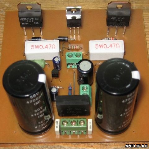
With a 4 ohm load, the amplifier delivers 150 watts; this is the cheapest and best option for a subwoofer amplifier. The amplifier circuit uses inexpensive rectifier diodes, which can be obtained at any electronic device.

The amplifier can provide such power due to the fact that composite transistors are used at the output, but if desired, they can be replaced with conventional ones. It is convenient to use the complementary pair KT827/25, but of course the amplifier power will drop to 50-70 watts. In the differential cascade, you can use domestic KT361 or KT3107.

A complete analogue of the TIP41 transistor is our KT819A. This transistor serves to amplify the signal from the differential stages and drive the outputs. Emitter resistors can be used with a power of 2-5 watts; they protect the output stage. Read more about the technical characteristics of the TIP41C transistor. Datasheet for TIP41 and TIP42.
PN Junction Material: Si
Transistor structure: NPN
Limit constant collector power dissipation (Pc) of the transistor: 65 W
Limit constant collector-base voltage (Ucb): 140 V
Limit constant collector-emitter voltage (Uce) of the transistor: 100 V
Limit constant emitter-base voltage (Ueb): 5 V
Limit D.C. transistor collector (Ic max): 6 A
Limit temperature p-n junction(Tj): 150 C
Cutoff frequency of current transfer coefficient (Ft) of the transistor: 3 MHz
- Collector junction capacitance (Cc): pF
Static current transfer coefficient in a common emitter circuit (Hfe), min: 20
Such an amplifier can be used both as a subwoofer and for wideband acoustics. The amplifier's performance is also quite good. With a load of 4 ohms, the output power of the amplifier is about 150 watts, with a load of 8 ohms the power is 100 watts, the maximum power of the amplifier can reach up to 200 watts with a power supply of +/-50 volts.